Reference Design for a 30W Power Supply with >91% Average Efficiency
Power Integrations offers its DER-631 reference design of a power supply intended for use as a USB wall outlet charger. The 30W output (selectable 5.1V / 6A or 9.2V / 3.3A or 15.3V / 2A) rail is designed for a high power USB charging with Type-A or Type-C ports.
The output utilizes INN3268C from the InnoSwitch3-CP family of ICs. This design shows high power density and efficiency that is possible due to the high level of integration of the InnoSwitch3-CP controller providing exceptional performance.
DER-631 is a low-line input flyback converter design. The key design goals were high power density, high efficiency, low no load consumption, and best in class thermal performance. This is intended for wall outlet USB chargers.
The InnoSwitch3-CP IC combines primary, secondary and feedback circuits in a single surface mounted off-line flyback switcher IC. The IC incorporates the primary MOSFET, the primary-side controller, the secondary-side controller for synchronous rectification and the Fluxlink™ technology that eliminates the need for an optocoupler needed on a secondary sensed feedback system.
Design Key Points
The design targets greater than 90% average efficiency for the 3 outputs. Efficiency was optimized with transformer design, chosen active devices and bias voltages. For the transformer design, it is best to keep the reflected voltage (VOR) low to decrease the RMS current on the secondary side. Lower VOR also means lower drain to source voltage on the primary side MOSFET that can reduce switching loss.
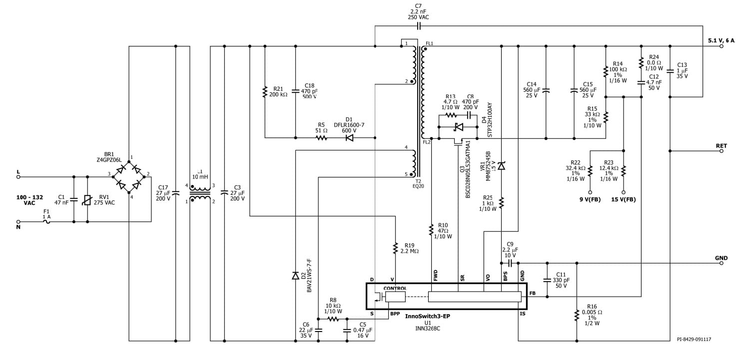 (click on schematic to enlarge)
In this design, the VOR was set to 50V for the 5V output. This will make the operation of the 5V output in continuous mode (CCM), but this will ensure the 9V and 15V output operations in discontinuous mode (DCM) with valley switching. InnoSwitch3-CP switches up to the 4th valley to achieve better efficiency.
This can trigger the SOA peak limit protection that will result to auto-restart. Aside from the VOR consideration it is also important to lower the leakage inductance of the transformer. The energy being stored in the leakage inductance which is dissipated on the clamping circuit contributes to lower efficiency.
Reducing the leakage is an utmost important in this design, to significantly increase the efficiency. A sandwich winding was used to lower the leakage inductance to a value less than 5μH (< 2% of magnetizing inductance).
For higher efficiency, it is also necessary to choose the active devices that offer lower conduction losses. For the InnoSwitch3-CP family, INN3268C offers the lowest RDS(on). For the secondary rectifier (SR), a MOSFET was chosen instead of a Schottky diode. A MOSFET of 2.8mΩ RDS(on) was used in the design.
An added Schottky diode in parallel with the SR MOSFET gives a slight improvement on the efficiency. This diode conducts instead of the MOSFET body diode during the start of secondary MOSFET ON and before the secondary current reaches zero or secondary MOSFET OFF. These delays on transition are needed to avoid cross-conduction with the primary MOSFET.
The sweet spot (efficiency and small form factor consideration) for switching frequency operation is at the range from 70kHz to 80kHz. An EQ20 transformer with AE of 60 mm2 is enough without saturating the core. The design chooses the minimum number of secondary turns at 390mT flux density.
Auxiliary bias voltage was chosen at range from 8V to 10V at no-load condition. This helps improves no load consumption as well as light load efficiency.

InnoSwitch™3-CP family features:
- Highly Integrated, Compact Footprint
- Up to 94% efficiency across full load range
- Quasi-Resonant (QR) / CCM flyback controller, 650 V or 725 V MOSFET4, secondary-side sensing and synchronous rectification driver
- Integrated FluxLink™, HIPOT-isolated, feedback link
- Supports fast charge protocols such as USB PD/QC 4.0
- Constant Power (CP) Profile minimizes charging time with continuous adjustment of output current and voltage
- Accurate CV/CC/CP, independent of external components
- External IS resistor allows custom CC programming
- Instantaneous transient response with 0%-100%-0% load step
- EcoSmart™- Energy Efficient
- Less than 15 mW no-load including line sense
- Easily meets all global energy efficiency regulations
- Low heat dissipation
- Advanced Protection / Safety Features
- Secondary MOSFET or diode short-circuit protection
- Open SR FET-gate detection
- Fast input line UV/OV protection
- Optional Features
- Cable-drop compensation with multiple settings
- Variable output voltage, constant current profiles
- Auto-restart or latching fault response for output OVP/UVP
- Multiple output UV fault thresholds
- Latching or hysteretic primary over-temperature protection
- Full Safety and Regulatory Compliance
- Reinforced isolation
- Isolation voltage >4000 VAC
- 100% production HIPOT testing
- UL1577 and TUV (EN60950) safety approved
- Excellent noise immunity enables designs that achieve class "A" performance for EN61000-4; EN61000-4-2, 4-3 (30 V/m), 4-4, 4-5, 4-6, 4-8 (100 A/m) and 4-9 (1000 A/m) and Ford FMC1278 (RI-115)