Three Things Engineers Should Consider When Using GaN and SiC in Power Electronics
By Matt Reynolds, Director of Product Marketing, Piezo and Protection Devices, TDK Electronics Inc.
Smaller, better, faster. These ideas are often pushed into new engineers' minds by executives. The same is true with the evolution of power electronics. Power semiconductors that are able to operate at increased switching frequency, allowing miniaturization through lower losses and therefore higher efficiency, require passive components with new characteristics, especially for capacitors. Dramatic reduction in the effective series inductance (ESL) and effective series resistance (ESR) of the capacitors are required in many of today's applications. To address these demands, new materials have been introduced that help switch higher power much faster and can reduce the size of the heat sink while keeping a high ripple current rating.
Design engineers should evaluate and implement new materials not only to receive performance enhancements, but also to increase the long-term reliability of power electronics. However, they must implement new technologies at the right time in order to ensure that the design is cost effective.
To do this, there are three things that engineers should consider when evaluating power electronics based on new materials:
- Thermal conditions, and therefore the cooling systems required
- Inductance and resistance, and the resultant effect on efficiency
- Total system cost, as opposed to one-on-one component cost comparison.
New Materials
This need for miniaturization and more efficient components with increased power handling requires that both semiconductors and passive components be made from different materials as well. Simply, when components are miniaturized, standard silicon, nickel, copper, traditional dielectric and magnetic materials can no longer handle the power requirements without losses so significant that the components significantly exceed their rated temperatures, shortening the life of the equipment.
Gallium nitride (GaN) and silicon carbide (SiC) are two of the newest materials that can be used in power electronics. They are described more generically as wide band-gap (WBG) semiconductors since the gap between valence bands and conduction bands is higher than that of silicon (Si) based semiconductors. The technological advance made possible by these materials helps to address the ever-evolving demand for smaller components, better performance, and efficient power consumption, ensuring lower lifetime cost of a design. For example, by many estimates, the lifetime energy costs to operate large server farms, now exceeds the initial capital expenditure.
 Components made from GaN and SiC are able to operate at higher junction temperatures than standard silicon
Thermal Conditions
GaN and SiC are able to operate at higher junction temperatures than standard silicon as a result of the wider band-gap, in the range of 2 to 4 electron-volts, as compared to 1 to 1.5 electron-volts for silicon. The result is an ability to operate at higher temperatures with a similar expected lifetime, or to operate at similar temperatures with a longer life. This provides the design engineer with two different design paths depending on the requirements of the application. Power electronics can be made much smaller, which will cause the components to operate at a higher temperature.
Alternatively, they can be designed to optimize cooling, either through natural convection or forced cooling, in a similar size compared to traditional designs, resulting in much longer operating life for the equipment. In addition, there are applications for severe environments where the ambient temperature is already excessive, requiring components that are able to operate efficiently at high temperature.
Higher Temperatures
This ability for semiconductors with new materials to operate at high temperatures requires the passive components surrounding them - the largest one being capacitors and inductors - to also operate at higher temperatures. Components that are made from new and improved materials will operate efficiently and achieve the performance needed, even at temperatures exceeding 175°C.
Wide-band semiconductor devices by their very nature often operate at higher temperatures as they switch at a higher frequency. This also means that the same - or more - electrical current is flowing through a smaller package, requiring a reduction in losses.
As a result, silicon carbide or gallium nitride would be used instead of silicon, and silver and copper would be used instead of nickel or tin. This enables smaller packages without excessive heating.
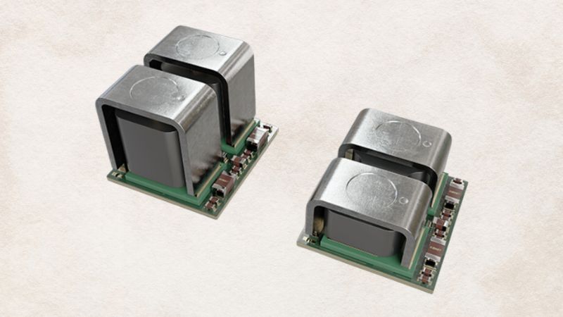
 Examples of different types of capacitors
All capacitors experience a degradation in isolation resistance at higher temperatures - the dielectric material start to break down, causing leakage current in the capacitor. This leakage current creates self-heating within the component, which heats it even more, ultimately causing failure. This self-heating condition is called thermal runaway.
The most commonly used power film capacitors utilize polypropylene, which is only rated at 105 °C maximum. This limits the types of end applications in which they can be utilized. Other, traditional capacitor materials, like aluminum electrolytic or Class 2 ceramics are able to operate at maximum temperatures of 125 °C to 150 °C, however, thermal runaway becomes a significantly higher risk. For higher temperature operation, new ceramic capacitor materials, such as PLZT, with lower leakage current at higher temperature would be required.
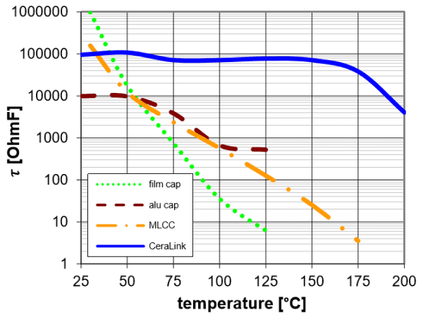 Insulation properties over temperature, capacitors with same voltage rating (click on graph to enlarge)
New Capacitor Technology
Even if a SiC semiconductor - that can go up to 150 °C or 200 °C - is utilized, traditional capacitor technology limits the conditions of the application. Capacitors based on lead lanthanum zirconate titanate (PLZT) ceramics, typically not only have a high permissible continuous operating temperature of 150 °C, but are often compact in design and have extremely low ESR and ESL values. PLZT capacitors are therefore ideal for fast-switching GaN or SiC semiconductors.
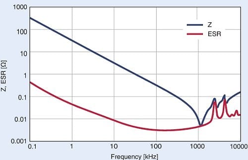 CeraLink ceramic performance over frequency (click on graph to enlarge)
GaN can switch as much as 1000x faster than standard silicon, at higher frequencies than its traditional counterparts. However, even though it operates at higher speeds, the new materials do not heat up as much as silicon. As a result, the cooling system can be smaller.
There are two basic types of cooling designs. The first is convection cooling which uses the circulation of air to cool the components. This can be passive convection where natural airflow is utilized or fans may be utilized for a forced air cooling. The second is liquid cooling, through the use of a circulating fluid. In either case, the components that have the highest thermal losses, are usually mounted directly to a heat sink to draw the excess heat generated from within the components. These are very often the power semiconductors and often the DC link capacitors as well. Because of their very nature, cooling systems are costly to implement and take up significant real estate in the design.
However, as electronics are miniaturized through the use of higher-temperature-capable materials, it is possible to obtain a higher power density without having to implement a more expensive cooling system in the design. While this should be considered during the design, often smaller components made from these new materials can operate without a cooling system and still maintain acceptable operating temperatures.
As a result, the consideration for engineers should be whether or not the design will support a higher temperature without employing drastic cooling measures as power density is increased.
Inductance and Resistance
Miniaturization in power electronics means higher power density. At the same rated voltages of the devices, this means higher currents for the same component size. Since there is no additional thermal mass, those components experience a greater degree of self-heating, resulting in higher operating temperatures. To offset this effect, new materials need to be used in the passive components, for example using pure copper inner electrodes for ceramic capacitors rather than nickel.
Copper has lower electrical resistivity, especially at elevated temperatures, compared to nickel, limiting the degree of self-heating. Novel processing techniques need to be employed for firing multilayer ceramic materials with copper inner electrodes. PLZT ceramic materials enable the use of copper inner electrodes under the right processing conditions.
Materials in and of themselves do not impact stray inductance, but rather, the geometry employed within the materials helps to reduce it. As a design is made smaller, it becomes denser. In general, as the physical dimensions become smaller the inductances naturally become smaller. Shorter lengths of wire, or shorter traces on PCB, and even smaller inductors and capacitors will have a tendency towards lower inductances.
It is also possible to even further reduce inductances by routing return current paths as close as possible to the supply path and in the opposing direction. The magnetic fields which result from the opposing currents cancel each other out and therefore lower the total system inductance. This places a burden on the design engineer to take care when laying out current paths, either cables, bus bars or traces on a circuit board to minimize these effects.
Total Cost
With the smaller size typically employed when new materials are used, there is simply less raw material used in the production of the part. And, as previously mentioned, if cooling systems are eliminated there is another possibility for cost reduction. As a result, over time volumes will increase and costs will be reduced. But until production processes are streamlined, they can have a higher upfront cost. The task for design engineers is to determine when to adopt the new technology.
While costs change from design to design, if the total cost of ownership is lower, even if the upfront costs are higher, the new technology will naturally be adopted.
Another cost-savings advantage is that new materials can be used to create significantly smaller components that can better handle increased switching frequency and better electromagnetic compatibility (EMC). The capacitances and inductances required for filtering common mode and differential mode interference are significantly smaller, and would use less material and therefore be lower in cost. The higher frequency of the emissions generated may require higher frequency dielectric and magnetic core materials, which might be higher cost materials, but should be more than outweighed by the dramatic reduction in size and weight of material.
Conclusion
With the availability of new materials to help enable the miniaturization of power electronics designs can accommodate higher power, higher-frequency switching and higher temperatures in a smaller package. As a result, engineers should consider the thermal conditions, cooling systems, inductance and the total lifetime cost of the design when designing their applications.
In many applications engineers will find that even though there may be a higher upfront cost, the overall lifetime cost of the design will be increasingly less expensive over time where miniaturized power electronics designs are needed. The trade-offs of enhanced performance, long-term reliability and lower maintenance costs over up-front costs will help these new materials see increased adoption as these material advances address new power electronics demands.