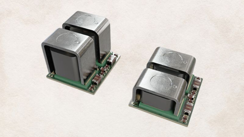
Toshiba America Electronic Components Inc. (TAEC, Irvine, CA) announced a new eight-pin, surface-mount package for use as a power MOSFET. Developed by Toshiba Corp. (Japan), the VS-8 is suitable for power management switching and dc/dc conversion in portable computers, portable phones, personal digital assistants and other emerging applications where space is at a premium.
The new VS-8 package has a 30 percent smaller footprint of 5.51mm² than its existing six-pin VS-6 package, and the thickness of the VS-8 package is 0.85mm, compared to similar packages currently available with a 1.1mm thickness. The package measures 1.9mm x 2.9mm x 0.8mm and weighs 0.011g. The Toshiba VS-8 package also features an improved power dissipation over the VS-6 package of 2.5W at t <5s, allowing use at a higher power output.
Utilizing Toshiba’s U-MOS III process technology, the VS-8 package features an on-resistance of 28mOhms at 4.5V (p-channel TPCF8101). Compared to Toshiba’s previous UMOS II process, the UMOS III reduces the on-resistance by 20 percent. To improve the device’s handling capability, the VS-8 includes a built-in zenar diode between the gate and source terminal for electrostatic discharge protection. The VS-8 line also includes a dual n-channel and a p-channel version in addition to an integrated p-channel and schottky barrier diode in a single package.
Samples of the VS-8 are currently available in the following functions: the TPCF8101 (single p-channel, -12V, -6A, 28mOhm at 4.5V), the TPCF8102 (single p-channel, -20V, -6A, 30mOhm at 4.5V), and the TPCF8301 (dual p-channel, -20V, -2.7A, 110mOhm at 4.5V). Volume production is slated for June 2002.