SiC-based High-Voltage Input 40W Auxiliary Power Supply Eval Board
The BD7682FJ-EVK-301 evaluation board from ROHM Semiconductor is a 40W auxiliary power supply that is able to operate with both ac and dc input voltages. It is therefore possible to derive the power directly from the grid or from the system dc link, for example, after the PFC stage. In case of ac input, the accepted input voltage range is 210Vac to 480Vac. In case of dc input, the input range is 300Vdc to 900Vdc.
This auxiliary supply provides an output of 12Vdc with regulation of ±3%. The board measures 80mm square. The simplified schematic of the BD7682FJ-EVK-301 evaluation board is shown above. It is designed for use in industrial applications.
This power supply is based on a flyback topology with a switching frequency of 90- to 120-kHz. Main devices used in this design are the SiC MOSFET SCT2H12NZ, with very low on resistance, and the quasi-resonant controller BDF768xFJ-LB. They enable a simple electrical and thermal design, reducing the number of devices, and avoiding the use of a heatsink for the flyback switch.
A custom transformer manufactured by Würth Elektronik has been used in this design. The primary side is composed by two windings in series, while the secondary side has been implemented with two windings in parallel. The half-windings are interposed, in order to reduce the leakage inductance around 1% of Lpri. This will impact the switching behavior of the MOSFET. In addition, the windings have been implemented with Litz wire to reduce the losses due to skin effect.
The efficiency of this power supply has been measured for three different input voltage values. The efficiency curves are shown below. As a dc power source was used, it was connected directly to the input capacitors. This way, the rectifying bridge is by-passed, saving the losses that would otherwise come from the bridge diodes. Efficiency is increasing with the output power, and it is higher for lower levels of input voltage. For and input of 300Vdc, the measured peak efficiency η=88% at POUT=33W - above that the overload protection was activated.
 Efficiency curves for several dc input voltages (click on image to enlarge)
The temperature of the main components of auxiliary power supply board has been measured, namely the SiC MOSFET (Q1), the Flyback transformer and the secondary diode (D20). The measurements were performed using an infrared camera. The thermal images are presented below. They were taken at room temperature, 800Vdc input and POUT=40W. The case temperature of the SiC MOSFET (Sp1) is around 84°C, even without the use of an external heatsink and without forced ventilation. The temperature of the flyback transformer (Sp2), registered on the winding corner, is slightly above 70°C. The measured temperature of the output diode (Sp3) was around 95°C.
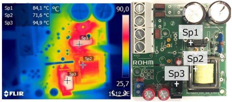 Temperature measurements from main components. (click on image to enlarge)
This board uses screw-type input connections to facilitate the cabling to 3-phase input or Vdc input. It is possible to remove the connectors and use vertical mounting connectors as an example of module-type auxiliary power supply in a power system.