SiC-Based 6.6kW Bi-Directional, Dual-Active-Bridge Resonant Converter Reference Design
The PMP21495 reference design from Texas Instruments is a 6.6kW, bi-directional, dual-active-bridge resonant converter design that accepts a 380Vdc to 600Vdc input and provides a 280Vdc to 450Vdc output. This design uses the C2000 micro-controller TMS320F280049 along with silicon-carbide (SiC) driver UCC21530-Q1 to drive bridges both on primary and secondary sides.
The design implements the daughter card approach to the C2000 controller (TMDSCNCD280049C) and SiC drivers (PMP21553 and PMP21561) and applies a Rogowski coil for synchronous rectifier (SR) optimization along with high bandwidth OpAmp LMV116MF. Possible applications include on-board and wireless chargers for automotive applications.
With 500kHz resonant frequency and 300kHz to 700kHz operational frequencies, this design is able to reach peak 98% efficiency. It includes over-current-protection (OCP) and over-voltage-protection (OVP) functions both at primary and secondary sides.
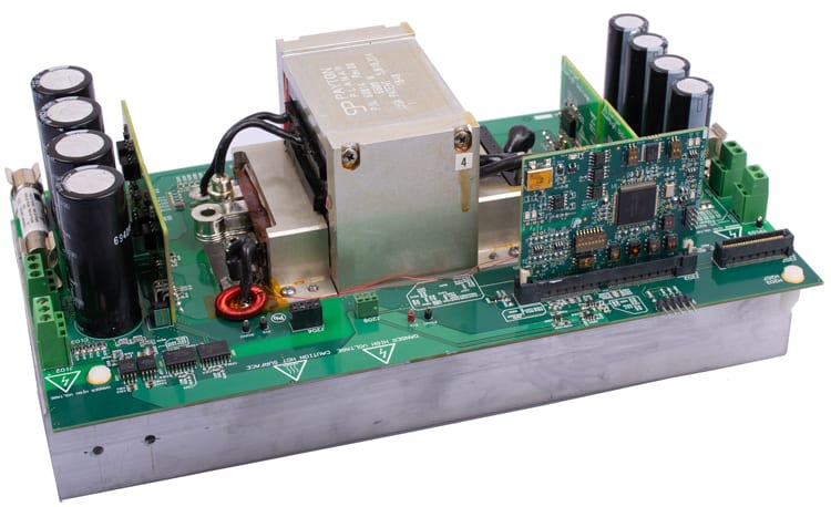 PMP21495 reference design
Features
- 500kHz resonant frequency, 300kHz to 700kHz operational frequency
- Capable of bi-directional energy flow
- Reach 98% peak efficiency at 280 V input
- Board dimension 5.8" x 10.7" x 3"
- High frequency, high voltage active synchronous rectifier control with Rogowski coil
UCC21530-Q1 Isolated Dual-Channel Gate Driver
This reference design features the UCC21530-Q1, an isolated dual-channel gate driver with 4A source and 6A sink peak current. The UCC21530-Q1 is designed to drive IGBTs and SiC MOSFETs up to 5MHz with best-in-class propagation delay and pulse-width distortion.
The input side is isolated from the two output drivers by a 5.7kVRMS reinforced isolation barrier, with a minimum of 100-V/ns common-mode transient immunity (CMTI). Internal functional isolation between the two secondary-side drivers allows a working voltage of up to 1850V.
 UCC21530-Q1 functional block diagram
This driver can be configured as two low-side drivers, two high-side drivers, or a half-bridge driver with programmable dead time (DT). The EN pin pulled low shuts down both outputs simultaneously and allows for normal operation when left open or pulled high. As a fail-safe measure, primary-side logic failures force both outputs low.
The device accepts VDD supply voltages up to 25V. A wide input VCCI range from 3V to 18V makes the driver suitable for interfacing with both analog and digital controllers. All the supply voltage pins have under voltage lock-out (UVLO) protection.
With all these advanced features, the UCC21530-Q1 enables high efficiency, high power density, and robustness in a wide variety of power applications.