The ISL71040MEV1Z evaluation platform from Renesas is designed to evaluate the ISL71040M. The ISL71040M is designed to drive enhancement mode GaN FETs in isolated topologies and boost type configurations. It operates across a supply range of 4.5V to 13.2V and offers both non-inverting and inverting inputs to satisfy non-inverting and inverting gates drive within a single device.
Applications are expected to include flyback and forward converters, boost and PFC converters, and secondary synchronous FET drivers.
The ISL71040M has a 4.5V gate drive voltage (VDRV) that is generated using an internal regulator that prevents the gate voltage from exceeding the maximum gate-to-source rating of enhancement mode GaN FETs. The gate drive voltage also features an undervoltage lockout (UVLO) protection that ignores the inputs (IN and INB) and keeps OUTL turned on to ensure the GaN FET is in an OFF state whenever VDRV is below the UVLO threshold.
The ISL71040M inputs can withstand voltages up to 14.7V regardless of the VDD voltage. This allows the ISL71040M inputs to be connected directly to most pwm controllers. The split outputs of the ISL71040M offer the flexibility to adjust the turn-on and turn-off speed independently by adding additional impedance to the turn-on/off paths.
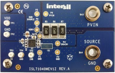 ISL71040MEV1Z evaluation platform.
The inputs stage can handle inputs to the 14.7V independent of VDD and offers both inverting and non-inverting inputs. The split output stage is capable of sourcing and sinking high currents and allows for independent tuning of the turn-on and turn-off times. A typical propagation delay of 36ns enables high switching frequency operation.
The ISL71040M offers a wide operating supply range of 4.5V to 13.2V. The gate drive voltage is generated from an internal linear regulator to keep the gate-source voltage below the absolute maximum level of 6V for the ISL7002xSEH GaN FET devices.
Key Features Include
- Wide VDD range
- 5V to 13.2V
- Location provided for load resistors to switch the GaN FET with a load
- SMA connector on the gate drive voltage to analyze the gate waveforms
- Drain/Source sense test points to analyze the drain to source waveforms
- Banana jack connectors for power supplies and drain/source connections
An example of a HEMT that the ISL71040M is designed to drive is the EPC2022 from Efficient Power Conversion, which offer very low RDS(on) and gate charge (Qg). These attributes make the devices capable of supporting very high switching frequency operation while avoiding significant efficiency loss.
However, GaN power FETs have special requirements in terms of gate drive that the ISL71040M is designed to specifically address. Key properties of a gate driver for GaN FETs are:
- Gate drive signals need to be sufficiently higher than the VGS threshold specified in GaN FET datasheets for proper operation
- A well-regulated gate drive voltage to keep the VGS lower than specified absolute maximum level of 6V
- Split pull-up and pull-down gate connections to add series gate resistors that independently adjust turn-on and turn-off speed. This eliminates the need of a series diode whose voltage drop can cause an insufficient gate drive voltage
- Driver pull-down resistance < 0.5Ω that eliminates undesired Miller turn-on
- High current source/sink capability and low propagation delay achieve high switching frequency operation