Quantum Physics of Paint-on Semiconductor Reveals Light and Solar Potential
A team led by researchers from the Georgia Institute of Technology have revealed the exotic physics behind the quantum particles of a unique composite material and their potential to transform lighting technology and photovoltaics. The researchers studied a sandwich of material made up of a hybrid of organic and inorganic Perovskites known as a HOIP for short. HOIPs are put together with many non-covalent bonds, making the material soft.
In the image above taken by Rob Felt, Carlos Silva in his lab at Georgia Tech with graduate research assistant Félix Thouin examine a setup to process laser light in the visible range for the testing of quantum properties in a halide organic-inorganic perovskite.
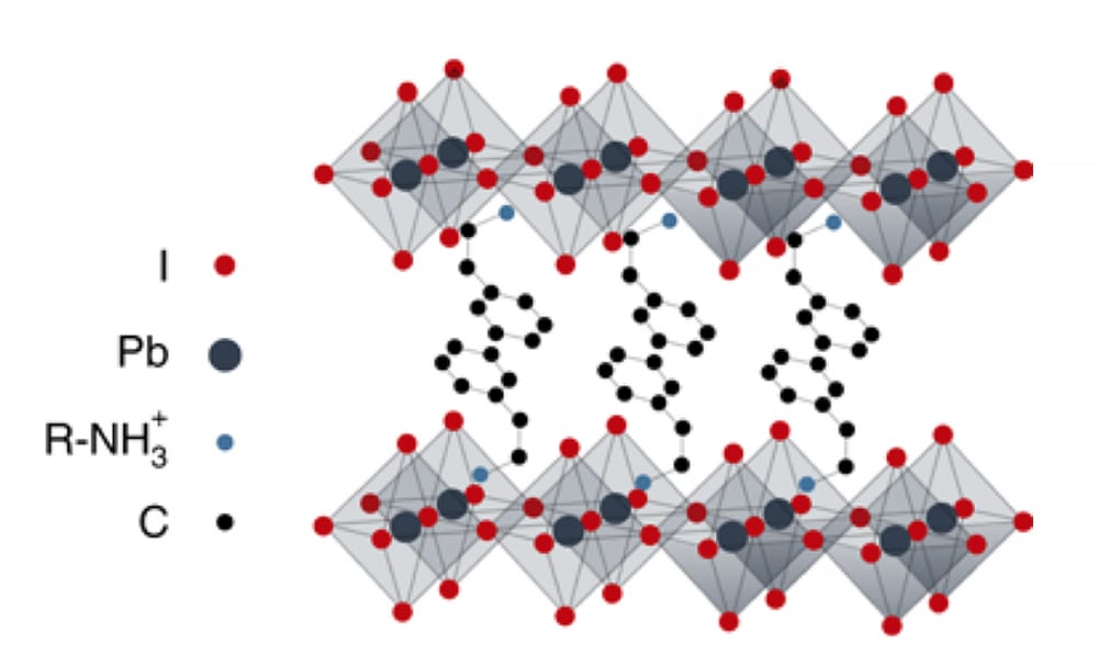
Individual units of the crystal take a form called perovskite, which is a very even diamond shape, with a metal in the center and halogens such as chlorine or iodine at the points, thus known as a "halide." For this study, the researchers used a 2D prototype with the formula (PEA)2PbI4.
Spinning groups of quantum particles ripple through the emerging materials, creating, highly desirable light and electronic properties, according to the research team of physical chemists. These same properties are extremely difficult to achieve in established semiconductors.
The particles moving through these new materials also involve the atoms of the material itself in the quantum action. The researchers were able to measure the patterns in the material resulting from the complex movements and relate them to the emerging material's quantum properties and the energy injected into the material. These insights could help engineers work productively with the new class of semiconductors.
Unusually flexible semiconductors
The emerging material's ability to house diverse and eccentric quantum particle movements is directly related to its exceptional flexibility on a molecular level and its non-covalent bonds which make it soft and flexible. By contrast, established semiconductors have rigid, lattice-like molecular structures.
Beyond the promise of their radiance and energy-efficiency, HOIPs are easy to make and apply. In fact, the material can be painted on.
 HOIP Molecular Model
"One compelling advantage is that HOIPs are made using low temperatures and processed in solution," said Carlos Silva, a professor in Georgia Tech's School of Chemistry and Biochemistry. "It takes much less energy to make them, and you can make big batches." Silva co-led the study alongside Ajay Ram Srimath Kandada from Georgia Tech and the Istituto Italiano di Tecnologia.
High temperatures are needed to produce most semiconductors in small quantities, and they are too rigid to apply to surfaces, but the researchers believe that HOIPs could be painted on to make LEDs, lasers or even window glass that could glow in any color from aquamarine to fuchsia. The team further speculates that lighting with HOIPs may need very little energy, and with the material solar panel makers could boost photovoltaics' efficiency and slash production costs.
Examination of Light Emission
Semiconductors in optoelectronic devices can either convert light into electricity as in solar cells or electricity into light as in LEDs. The researchers focused on processes connected to light emission.
One way to get a material to emit light is to apply energy to the material's electrons so that they take a quantum leap up from their orbits around atoms. Then the electrons emit that energy as light when they drop back down to the orbits they had vacated.
Established semiconductors can trap electrons in regions of the material that stringently limit the electrons' range of motion then apply energy to those areas to make electrons do quantum leaps in unison to emit useful light when they drop back down together.
"These are quantum wells, two-dimensional parts of the material that confine these quantum properties to create these particular light emission properties," Silva said.
The hybrid semiconductor material has a potentially more attractive way to produce the light. An electron has a negative charge, and an orbit it leaves after having been excited by energy is a positive charge called an electron hole. The electron and the hole can revolve around each other forming a kind of imaginary particle, or quasiparticle called an exciton.
"The positive-negative attraction in an exciton is called binding energy, and it's a very high-energy phenomenon, which makes it great for light emitting," Silva said.
When the electron and the hole reunite, that releases the binding energy to make light. However, usually, excitons are very hard to maintain in a semiconductor.
"The excitonic properties in conventional semiconductors are only stable at extremely cold temperatures," Silva said. "But in HOIPs the excitonic properties are very stable at room temperature."
Complex quasiparticle twirling
Excitons get released from their atoms and move around the material. In addition, excitons in a HOIP can whirl around other excitons, forming other quasiparticles called biexcitons.
Excitons also spin around atoms in the material lattice. Much the same way an electron and an electron-hole create an exciton, this whirling of the exciton around an atomic nucleus gives rise to yet another quasi-particle called a polaron. All this action can result in excitons transforming into to polarons back. Some excitons are known to even take on a "polaronic" nuance.
Complicating all those dynamics is the fact that HOIPs are filled with positively and negatively charged ions. The ornateness of these quantum dances has an overall effect on the material itself.
Wave patterns resonate
The extraordinary participation of the material's atoms in these patterned movements with electrons, excitons, biexcitons, and polarons creates repetitive nanoscale indentations in the material that are visible as wave patterns that shift and flux with the amount of added energy.
"In a ground state, these wave patterns would look a certain way, but with added energy, the excitons do things differently. That changes the wave patterns, and that's what we measure," Silva said. "The key observation in the study is that the wave pattern varies with different types of excitons (exciton, biexciton, polaronic/less polaronic)."
The indentations also seize the excitons, reducing their mobility through the material, and all these elegant dynamics may affect the quality of light emission.
The team led by Georgia Tech included researchers from the Université de Mons in Belgium and the Istituto Italiano di Tecnologia. The results were published on January 14, 2019, in the journal Nature Materials. The work was funded via the U.S. National Science Foundation, EU Horizon 2020, the Natural Sciences and Engineering Research Council of Canada, the Fond Québécois pour la Recherche, and the Belgian Federal Science Policy Office.