Next-Gen GaN-on-SiC Power Devices from New Epi Growth Mechanism
SweGaN AB has collaborated with top scientists from Linköping University in Sweden and The Institute of Electronics, Microelectronics and Nanotechnology (IEMN), a French research group dedicated to high power devices, and has developed new epitaxial growth mechanism, Transmorphic Heteroepitaxy, for producing next generation gallium-nitride on silicon-carbide (GaN-on-SiC) power electronics.
Illustrated above, GaN and AlN epitaxial layers grown by SweGaN's high-temperature process exhibit excellent structural quality. Typically, the threading dislocation density in the GaN layer is in low 108cm-2 regime and the AlN nucleation layer is free of grain boundaries. This is the best structural quality in the class, which not only guarantees the GaN robustness but also dramatically reduces the risk of device failure due to the structural defects.
The new hybrid GaN-on-SiC material promises significant power savings in hybrid and electric vehicle drive trains, EV chargers, as well as photovoltaic solar inverters and other high-power applications.
SweGaN collaborated with the scientists in electron microscopy and modeling from Linköping University, Sweden and the senior researchers from IEMN in France to explore the nature of the new epitaxial growth mechanism and the potential of SweGaN's QuanFINE® heterostructures for high power applications.
QuanFINE™ structure is built on the concept of a GaN-SiC hybrid material, that combines the high-electron-velocity thin GaN with the high-breakdown bulk SiC, which has been realized by SweGaN's revolutionary MOCVD process and proven to be competent for the use in both high-frequency and power transistors. For high-frequency applications, QuanFINE™ features a buffer-free HEMT heterostructure, where the AlN nucleation layer serves effectively as a back-side barrier. Therefore, the electrons in the thin GaN channel (<250nm) are well confined in the quantum-well-like structure by the front-side and back-side barriers.
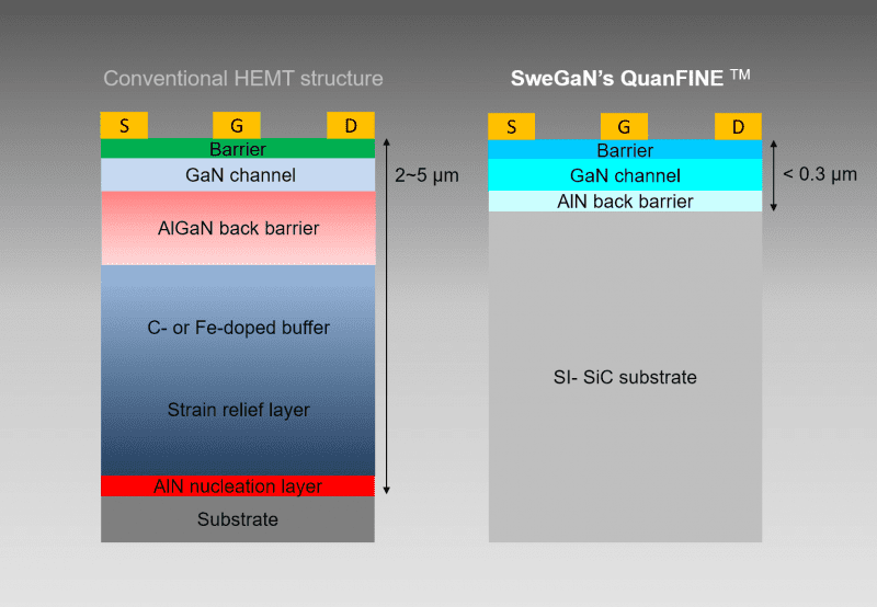
For power applications, QuanFINE™ utilizes the semi-insulating SiC substrate as the voltage blocking layer, the quality and resistivity of which is significantly higher than the conventional thick carbon-doped GaN buffer layer. Moreover, it also offers the best thermal management in the class, resulting from the nearly perfect GaN-SiC interface.
According to SweGaN, these newest findings place the company in the forefront of heteroepitaxy technology for producing QuanFINE®, a hybrid GaN-SiC material for manufacturers of power devices - in addition to its current product portfolio for RF components and devices.
"Not only is this a high-impact innovation, but comes together with a scientific discovery of a novel epitaxial growth mechanism, what we coin transmorphic, " says Lars Hultman, co-author of the publication, and professor at Linköping University and member of the Royal Swedish Academy of Sciences.
"This breakthrough could significantly reduce the power loss for high power devices, which would truly manifest the superiority of GaN power devices over Si super-junction power devices and SiC MOSFETs for 650V rated devices", says Jr-Tai Chen, CTO at SweGaN AB.
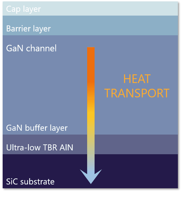
Ultra-Low Thermal Boundary Resistance
The conventional Thermal Boundary Resistance (TBR) in the GaN - SiC interface causes up to 40% additional channel temperature rise in transistors. Using our ultra-low-TBR AlN nucleation layer, we have been able to reduce this additional temperature rise to a negligible level. The outstanding structural quality of the thin AlN nucleation layer significantly improves the heat transport from the channel down to the high-thermal-conductivity SiC substrate. This allows us to address one of the biggest challenges with RF and power devices: reliability. By reducing the operational temperature by 25 °C, the device lifetime is increased by a factor of 10.
Summary of key findings from the joint collaboration
The newest groundbreaking results show an epitaxial growth - Transmorphic Heteroepitaxy - where less than 1nm-thin atomic interlayers with ordered vacancies are made to sufficiently accommodate the lattice mismatch at the interface between the first epilayer and the substrate.
- This new growth mechanism suppresses the formation of structural defects in the beginning of the epitaxy, which enables grain-boundary-free AlN nucleation layers and subsequent high-quality buffer-free GaN-based heterostructures to be realized on SiC substrates.
- A GaN HEMT heterostructure with a total thickness less than 300nm grown by the transmorphic epitaxial scheme on a semi-insulating SiC substrate shows a lateral critical breakdown field of about 2MV/cm and a vertical breakdown voltage of ≥3kV, measured by the senior researchers at IEMN.
- The critical breakdown field is nearly 3-times higher than that of GaN-on-Si epiwafers grown by the conventional thick-buffer approach. This means that the device ON-resistance has potential to be lower by >1 order magnitude than the value achievable today, according to Baliga's Figure of Merit.
"With these new results, SweGaN will now extend focus of its QuanFINE® technology to include the global power market in addition to RF devices for satellite, communications and defense organizations, particularly in Asia showing the most hunger for new generation GaN power devices," continues Jr-Tai Chen. "We anticipate releasing more new findings on the performance of QuanFINE® based power devices in the near future."
Key research from a project funded by the EU Horizon 2020 research and innovation program (grant agreement no. 823260) was an important contribution to the new development.
Latest findings from the research collaboration and details of the joint teams will be published on November 25th as a Featured Article in Applied Physics Letters, and in Volume 115, Issue 22, of APL: "Transmorphic Epitaxial Growth of AlN Nucleation Layers on SiC Substrates for High-Breakdown Thin GaN Transistors."