Imec Demonstrates Monolithic GaN Half-Bridge with Drivers in 48-V to 1-V Buck
At PCIM 2019, imec demonstrated a functional GaN half-bridge monolithically-integrated with drivers. Mounted on a buck-converter test board, the chip converts an input voltage of 48V to an output voltage of 1V, with a pulse width modulation signal of 1MHz. The achievement leverages on imec's GaN-on-SOI and GaN-on-QST® technology platforms, reducing parasitic inductance and boosting commutation speed.
Today, GaN power electronics are dominated by off-the-shelf discrete components. Half-bridges -common subcircuits in power systems - are fabricated by separate discrete components, either in separate packages, or integrated in one package, especially for the higher voltage ranges.
Realizing half-bridges on chip by using GaN-on-Si technology, is very challenging, especially at high voltages. This is because half-bridges designed on GaN-on-Si technology are limited in performance by a back-gating effect that negatively affects the high-side switch of the half-bridge, and switching noise that disturbs the control circuits.
To unlock the full potential of GaN power technology, imec monolithically co-integrated a half-bridge and drivers in one GaN-IC chip. Complemented by low voltage logic transistors, a suite of passive components for low-ohmic and high-ohmic resistors, and a MIM-capacitor, high-end integrated power systems can be realized on one single die.
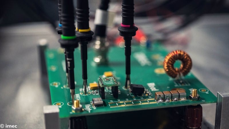 Evaluation board
Imec's solution builds on imec's GaN-on-SOI and GaN-on-QST® technology platforms that allow for a galvanic isolation of the power devices, drivers and control logic, by the buried oxide and oxide-filled deep trench isolation. This isolation scheme not only eliminates the detrimental back-gating effect that negatively affects the high-side switch of the half-bridge, but also reduces the switching noise that disturbs the control circuits.
With the design of a co-integrated level shifter for driving the high-side switch, a dead-time controller to avoid overlapping gate input waveforms, and an on-chip pulse-width modulation circuit, highly integrated buck and boost convertors can be fabricated.
"Someone might think that by using SOI or QST® wafers instead of Si wafers will result in more expensive technology. However, with GaN-on-Si several discrete devices need to be individually packaged (with advanced packages to take advance of the GaN fast switching performance) and connected to their drivers and other elements at the board or packaged level", stated Denis Marcon, business development manager at imec.
"Instead, with imec's GaN-IC technology, the full converter including drivers and analog blocks etc. is on-chip, which can then be packaged with simple package technology (as the frequency sensitive components are already connected on-chip). This dramatically saves on the cost of the final power system," added Marcon.
To further boost the performance of these monolithic integrated power systems, imec aims to extend its platform with additional co-integrated components, such as Schottky diodes and depletion-mode HEMTs.
"With the aim to further foster innovation in the GaN power electronics, this GaN-IC platform is available for prototyping through our multi-project-wafer (MPW) service", commented Stefaan Decoutere, program director GaN power electronics at imec.
"The possibilities for high-end power systems with unprecedented performance, either in switching speed, operating frequency or energy efficiency, with reduced inductive parasitics and unseen reduction of the form-factors, will further boost the use of GaN for power supplies in the consumer and re-useable energy market segments," Decoutere concluded.


