Fraunhofer IZM to Present Wide Bandgap Technologies and Services at PCIM Europe 2019
Fraunhofer IZM will again be presenting at PCIM Europe 2019 in Nürnberg at Booth 437/Hall 7.
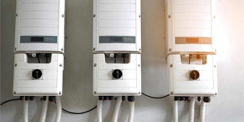
At PCIM 2019, Fraunhofer IZM will be showcasing its entire range of services from in the realm of power electronics. The services being showcased covering everything from system design and packaging technologies for power electronics to reliability characteristics and cooling concepts. (The image above shows a miniaturized, zero-dead-time high-efficiency driver for Si, SiC, and GaN applications, © Fraunhofer IZM).
Measuring switching losses in wide bandgap semiconductors
The traditional approach for measuring switching losses like double pulses is based upon measuring the current in the semiconductor and the voltage drop at the point of switching. However, the parasitic effect of the measuring equipment itself can skew the measurements.
Several methods have been developed to overcome this issue and measure switching losses passively under realistic working conditions. They allow an accurate assessment of switching losses at various currents, voltages, and temperatures without needing any modification to the switch cell itself. This method makes an accurate measurement of even fully integrated modules possible.
Christoph Marczok's paper titled, "Low Inductive SiC Mold Module with Direct Cooling" is honored with the Young Engineer Award of the PCIM Europe 2019.
 Christoph Marczok (© Fraunhofer IZM)
Making use of the superior properties of wide-bandgap semiconductors requires that power modules have excellent electromagnetic properties, the ability to operate at high temperature, and a design that allows a high degree of integration.
Christoph Marczok's paper discusses a new setup for power modules with SiC power MOSFETs using multilayer ceramic substrates with direct substrate water-cooling. Transfer molding with a metalized and structured copper layer on top encapsulates the power modules. Then, SMD components are soldered directly on this metallization. Finally, the paper includes the double pulse switching results of the power module.
The paper is co-authored by Prof. Eckart Hoene (Fraunhofer IZM), Tina Thomas (Fraunhofer IZM), Andreas Meyer (Rogers Germany GmbH) and Karsten Schmidt (Rogers Germany GmbH).
The award ceremony will take place at the opening session of the PCIM Europe Conference on 7 May 2019 in Nuremberg.
Miniaturized, Zero-Dead-Time High-Efficiency Drivers for Si, SiC, and GaN Applications
A new Fraunhofer IZM concept reveals new approaches for reducing switching losses of fast-switching power semiconductors by eliminating the effect of the freewheeling diodes.
The first step is recovering the energy stored in the gate to reduce the energy consumption of the driver. This energy recovery is achieved by moving from resistive to inductive gate current controls, which showed itself to be a feasible approach.
Reduced power consumption enables the second step of the concept. By transferring energy to the high side via a 10pF capacitor at high frequency (70MHz), standby supply can be kept to a minimum.
As an additional feature, a new means of eliminating dead time was investigated. This dead time elimination was accomplished by coupling high and low side gate paths via a transformer. This was also shown to be an effective method for reducing switch losses and significantly decreasing ringing effects.
Low Inductance
Silicon carbide semiconductors offer a high current slope during turn-on and turn-off. This high current slope can be used for a significant increase in switching frequency.
While switching losses can be reduced, at the same time, over-voltages during turn-off, which occur due to the inevitable parasitic package inductances, become more considerable. These overvoltages can destroy the chip and result in further ringing, which increases switching losses.
In the project presented, two modules were built up and compared to each other; one conventional style, with wire bonds for chip contacts and broad busbars to connect the dc-link, and one embedded module.
For the latter, chips were soldered onto a DCB in a standard process, but the dc-link was connected via a busbar realized in PCB technology. The DCB ensures a much better thermal performance than a polymer.
Part of the dc-link capacitors are situated on the module.
A current slope of up to 4A/ns and only little over-voltage and ringing during turn-off can be achieved that way. Commutational inductance is just 0.866nH.
Commercially available current measurement systems could not provide an accurate switching-current measurement. So, an inductive shunt was developed to characterize the module.
Packaging for Power Electronics
Besides die attach soldering and Al-heavy wire bonding, new packaging concepts were pursued to built power electronics systems which provide improved thermal performance and higher reliability. Replacing the wire bond with an area contact on both sides of the chips can improve the thermal performance.
Silver sintering is one of the new die attach technologies, which result in an increased lifetime of the whole power package. Silver is ductile, meaning that it has a high melting point and a very high thermal conductivity. Therefore, especially for a higher performance and higher operating temperatures, Ag sinter joints are very promising.
Another new joining technology currently under development is referred to as "transient liquid phase soldering" or "bonding" (TLPS or TLPB). The idea behind this technology is that the Sn-based solder is transformed in intermetallic phases which have a higher melting temperature than the solder alloy had before the joining was carried out. The higher melting point is necessary to withstand higher operating temperatures or for withstanding subsequent soldering processes during manufacturing.
The lifetimes of wire or ribbon bonds may also be improved. Using Cu wire instead of Al reduces the thermal mismatch between the Si die and the wire bond material. In order to use Cu bonds, the power chips have to have a Cu metallization on top. The IZM can deposit Cu layers on semiconductor wafers using electroplating.
Lastly, an encapsulation material is applied to the power package. This can also be done at the Fraunhofer IZM.
Compact Converters Enabling High Power Density
Due to the low switching losses when using the novel wide band-gap semiconductor generation made from gallium nitride and silicon carbide, respectively, it is possible to increase the switching frequency of power electronic systems significantly. As a result, the size of passive components, especially of the bulky ripple inductors, can be reduced because less energy needs to be buffered in the system.
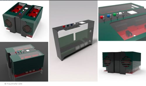 Compact converters that enable high power density
The focus of the ECPE lighthouse project "Industrial Demonstrator on System Level" is about using innovations in filter topology and semiconductor control to provide an additional power density increase.
The control system gathers all measured values simultaneously and regulates the duty cycles of all six half bridges. Both gate signals inside a half bridge are magnetically coupled. As a result, switching between top and bottom semiconductor realizes zero dead time switching, and the switching losses can be further reduced.
Due to the very high temporal accuracy of the control signals of less than 500ps the required additional gate charge can be adjusted precisely and oscillations with the gate-source capacitance can be avoided. The operation parameters can be transmitted using various interfaces (USB, CAN-Bus and Ethernet) or directly adjusted on the control panel.
According to the electrical load conditions, the control system supports the application of different operation modes (DCM, CCM, flat top modulation) during one mains period and rotary field period, respectively. In this way, the die voltage-time-area of the PFC and motor inductors and thus, their size, can be further reduced. Shifting the CM voltage into the DC link achieves the size reduction of the CM filter.
Ultimo - Ultra-Compact, Ultra-Reliable Power Module
Fraunhofer IZM is working with automotive manufacturers and suppliers to design and manufacture an ultra-compact power module with double-sided cooling for high power density applications.
This work collaboration is being done as part of an industry-based research consortium on "Improving energy efficiency using power electronics," which is funded via the German federal ministry of education and research (BMBF).
The module, which will be integrated into an existing inverter once the development has been completed, is comprised of semiconductors sandwiched between two DCBs. Water cooling by cooling bodies, with the cooling agent guided across each side of the module, maximizes thermal dissipation and minimizes overall thermal resistance.
The development work employed innovative interconnection techniques such as transient liquid phase bonding (TLPB). With TLPB, a solid, temperature-resistant, yet thin interconnection layer can be achieved between a chip and substrate. Apart from improved stability, the technique ensures that the packaging no longer limits the maximum chip temperature.
Ultra Low Inductive Multilayer Ceramic SiC Power Module
Power Module Design
This ultra-compact low-inductive power module design contains many innovations, which allow a high power density combined with an excellent electrical performance. The design is based on a curamik® multilayer ceramic substrate supplied by Rogers Corporation with two electrical layers on top and in the middle.
The insulated bottom copper layer contains an integrated heat sink. In spite of two ceramic layers, a very low thermal resistance below 0.265K/W from junction to fluid can be reached.
The assembly is molded after sintering the SiC MOSFETs onto the ceramic substrate. On top of the mold cap, a structured electrical copper layer is implemented and electrically connected to the substrate with drilled blind vias. The combination of the innovative substrate, the additional electrical layer on the mold cap, and the integration of a local DC-Link on-board offer a very low inductive commutation cell design with Lσ < 2nH.
It also allows for a very low inductive DC+ / - input connection, an implementation of SMD components and consequently a first on-board driver stage with lowest parasitic stray inductance in the gate path to the chip.
Packaging Technologies
SiC Chip Assembly on Substrate
- High precision & tilt-free assembly (+/- 10μm in x/y/z)
- Sintering of prepackaged SiC chip on copper surface
- Encapsulation
Transfer Molding Technology
- Encapsulant suitable for subsequent via lasering
Encapsulation of thick substrate (4.5mm) with challenging filling geometry
Redistribution & SiC Interconnection
Direct Metallization of Molding Surface
- Laser drilling of blind vias in epoxy molding compound (400μm/1000μm)
- Surface finish according to subsequent SMD assembly
SMD Assembly
- State-of-the-art lead-free soldering of SMDs
APPLICATIONS
To make use of the superior properties of Wide Band Gap (WBG) semiconductors power modules are needed with optimized parasitic electromagnetic properties and high temperature capability, furthermore with the possibility for a high degree of integration:
Requirements on Wide Bandgap Power Modules
- Low inductive commutation cell,
- Low inductive gate path,
- Low inductive input connectors,
- Very low thermal resistance.
Advanced Low Inductive Power Modules Provide Unique Features
- Lowest possible switching losses,
- A low RDS(on),
- Nearly no voltage overshoot while turn-off,
- More output power out of the same chip,
- Reduction in size and weight.
- Thus, they are interesting for a wide range of automotive, solar energy and industrial applications.
Technical Data
Electrical characteristics
- Half-bridge design
- Uds,max = 1200V
- RDS(on) = 11mΩ
- Iout,eff = 160A
- Power range up to 50kW (150kW for 3 phases)
- Local DC-Link on-board
- SMD components on-board
- Driver booster on-board for lowest gate inductance
- Lσ, power module < 2nH
- Thermal characteristics
- Integrated heatsink in the ceramic substrate
- Insulated heatsink
- Single sided cooling
- Rth(junction-fluid) ≤ 0.265K/W
- Mechanical characteristics
- Ultra-compact design
- Size: 48mm x 48mm x 5mm + SMD components and frame
- Multilayer Si3N4 ceramic substrate
- Spring contacts (Load and driver)