Eval Board for SiC MOSFET Modules in a 22.5kW Bidirectional Buck-Boost Converter
The EVAL-PS-E1BF12-SiC board from Infineon Technologies is designed to enable the evaluation of the company's FF11MR12W1M1_B11 and F23MR12W1M1_B11 CoolSiC™ silicon carbide MOSFET modules in a bidirectional buck-boost converter topology with a maximum output power of 22.5kW. This evaluation board allows users to evaluate the device performance via double-pulse measurements and functional tests.
The EVAL-PS-E1BF12-SiC board is designed to assist in the development of power converters for use in solar energy systems, uninterruptible power supplies, EV battery chargers, and similar applications.
SiC MOSFET-based modules are a revolutionary step towards highly efficient power electronic devices with a benchmark in terms of power density. Switching frequencies exceeding 100kHz as well as greater than 99% power conversion efficiency are simple to implement using Infineon EasyPACK™ modules with CoolSiC™ trench-MOSFET devices.
You may also like: Cree and STMicro Expand and Extend SiC Wafer Supply Agreement
Using the EVAL-PS-E1BF12-SiC evaluation board, engineers can evaluate these devices:
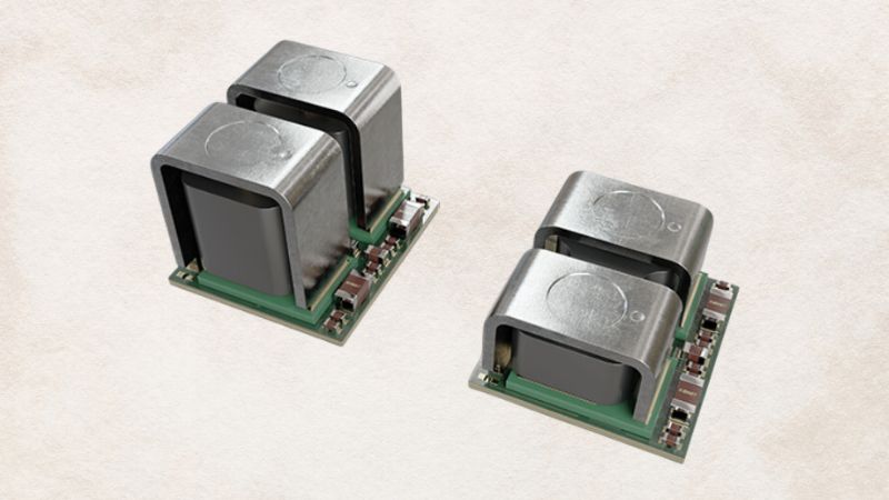
- The FF23MR12W1M1_B11 is an EasyDUAL™ 1B 1200V, 23mΩ half-bridge module with CoolSiC™ MOSFET, integrated NTC temperature sensor and PressFIT Contact Technology.
- The FF11MR12W1M1_B11 is an EasyDUAL™ 1B 1200V, 11mΩ half-bridge module with CoolSiC™ MOSFET, NTC and PressFIT Contact Technology.
The main function of this board is the evaluation of the FF11MR12W1M1_B11 and the FF23MR12W1M1_B11 modules in combination with the EiceDRIVER™ 1EDI60IH12AH driver. Electrical or optical pulses are translated in the evaluation board to signals for the 1EDI60IH12AF driver. Each driver controls one of the SiC MOSFET switches within the FF11MR12W1M1_B11 or FF23MR12W1M1_B11 modules. The driving voltages are -3V/18V.
Summary of capabilities and functionality:
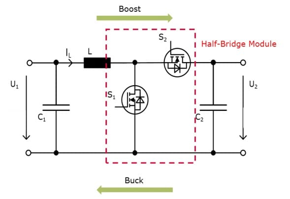
- A bidirectional buck-boost converter is a useful converter in today's power electronics' world. As an example, transformer-less chargers use it to charge and discharge high-voltage batteries. Another application for the boost mode is the maximum power point tracker for PV applications achieving high efficiency by synchronous rectification. Referring to the above image: In the boost operation mode, S1 is the active switch, while S2 is operated as the diode. The buck operation works with S2 as the active switch and S1 as the diode.
- The evaluation board is electrically and mechanically suitable for the FF11MR12W1M1_B11 and the FF23MR12W1M1_B11 CoolSiC™ MOSFET modules. The initial configuration of the board is equipped with the required components to do:
- Double-pulse characterization
- Functional testing of the buck-boost operation using electrical loads at the input or output stage