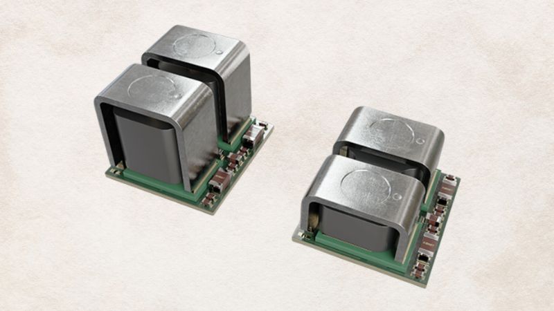
In power supplies that are used for server, telecom, and industrial applications there is typically a small bias power supply in addition to the main power converter. The KIT_6W_12V_P7_950V from Infineon Technologies is a 6W bias board designed to run in a system where it is continuously powered from the 400Vdc output of a boost power factor correction (PFC) converter and provides power to the fan, gate drivers, and controller.
This board uses the ICE5QSAG quasi-resonant (QR) flyback controller and the new 950V CoolMOS™ P7 (IPU95R3K7P7). This 950V breakdown voltage gives additional margin in the system to ensure the bias continues to run through surge events. This design was done as a snubberless flyback converter to further improve the efficiency over the entire load range.
The performance of the new design (with 950V CoolMOS™ P7) compared to the old version (with 800 V CoolMOS™ C3) can be seen in the figure below. The efficiency improvement is between 9.6 percent and 27.0 percent over the 1W to 6W load range, shown by the red line. The underside of the new bias board can be seen, along with the reduction in the overall form factor.
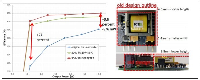 The improvement in efficiency at 400Vac and the form factor (click on image to enlarge)
It can also be seen that by changing from 800 V CoolMOS™ P7 to 950 V CoolMOS™ P7 there is an efficiency gain by reducing the VDS capacitor for snubberless operation from 100pF to 10pF, which helps to reduce the overall switching losses of the system. The 950V CoolMOS™ P7 also helps to increase the MOSFET breakdown voltage margin of the design to 20.6 percent margin.
Summary of KIT_6W_12V_P7_950V features
- Quasi-resonant flyback using a Infineon's second generation controller
- Snubberless operation to improve efficiency
- 950V breakdown voltage allows operating off of higher input voltages
- Primary side regulated 12V and a secondary side unregulated 12V output
Summary of benefits
- High efficiency
- Low cost solution
- Reduced PCB hotspot due to elimination of the snubber network