1.7kV SiC JFET Eases High Voltage Utility Power Supply Design – App Note
By Mike Zhu, UnitedSiC
The emergence of fast switching silicon-carbide (SiC) wide bandgap (WBG) devices has dramatically enhanced power density in a range of power conversion circuits such as active rectifiers, LLC bridges, phase-shifted full bridges, and dual active bridges, to name a few. These circuits form the backbone of efficient ac-dc and dc-dc stages in battery chargers for EVs, forklifts, solar inverters and power supplies, especially where power density is key.
Besides higher power density, SiC is also appealing for high-voltage applications such as energy storage, solar inverters and high voltage traction etc. For these applications the dc voltage can be easily above 1000Vdc and ac voltage can range from 480Vac to 530Vac. Such high power and high voltage systems are typically controlled by circuitry that utilizes much lower voltages. Microprocessors, communication protocols, cooling fans and sensors require a variety of low voltages.
A common approach to generate these voltages is with the flyback topology. However, most Si-based devices have lower design margin for voltage stress compared to SiC devices. Using Si-based devices may negatively impact reliability of the flyback converters which is crucial to the safe operation of the above mentioned high-voltage applications. Moreover, SiC devices have lower on-state resistance (Rdson) and faster switching speed which leads to higher efficiency.
UnitedSiC has pioneered the introduction of SiC JFET based FETs with easy drop in compatibility with Si MOSFETs, IGBTs as well as SiC MOSFETs, based on the 5V threshold voltage and wide gate operating range of +/-25V. These devices are inherently very fast switching, with excellent body diode characteristics.
In this application note, a discrete 1.7kV SiC JFET together with a 30V Si MOSFET in the cascode configuration is used as the main power switch in a flyback utility power supply. The JFET not only provides good efficiency, but also simplifies the startup circuitry by doubling as the startup circuit's high voltage pass element. [1][2][3]
Flyback Converter
In Figure 1 below is the top-level schematic of the utility supply that is implemented in this application note. A wide Input voltage of 200V to 1000V generates regulated output voltages of +12-, -12- and +5-V.
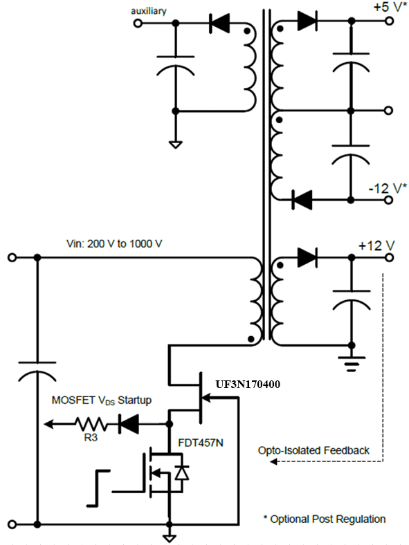 Figure 1. Flyback Converter with ±12V, +5V Outputs.
In this implementation, the +5V and the -12V outputs are low current (< 1 Amp), and have the option of a SOT-223 LDO post regulator. Unless noted, an LDO is utilized on the +5V output, and the -12V is regulated per the +12V output in all efficiency measurements.
The +12V output is directly regulated through a TL-431 opto-coupler to a UCC38C41 pwm controller to maintain tight regulation, while providing good primary to secondary isolation.
The printed circuit board was laid out to accommodate a wide range of loads, so modifications can be made to meet different specifications.
Power Switch
The power switch comprises a 400mΩ, 1.7kV SiC JFET (UF3N170400) paired with a 60mΩ, 30V Si MOSFET in a cascode configuration. The low voltage MOSFET can be driven with a standard drive (0V to 10V). Therefore, one can take advantage of silicon carbide without having to provide negative gate drive, or high gate voltage (>18V) to switch the device, as is the case with SiC MOSFETs.
Startup Circuit
One of the unique advantages of the cascode is its simplification of the converter's startup. In a typical high voltage startup circuit, a second high voltage device is needed to provide +12V to power the controller along with bias resistors that continue to dissipate power after the converter is operating. Using a high voltage JFET in this cascode configuration, that issue is solved. With the cascode in the off state at startup, the MOSFET drain voltage will stay at approximately the inverse of the JFET threshold voltage. This voltage can be used to power the converter's control circuitry until the auxiliary winding is regulating. In Figure 1, a resistor and diode are used to connect the MOSFET voltage to the control circuity.
To successfully implement this startup, several conditions need to be met. The most critical item is the under-voltage lockout (UVLO) of the control circuitry. The UVLO of the control circuitry has to be lower than the JFET threshold absolute value, otherwise this startup circuit won't work. In this design an UCC38C41 with a UVLO of 7.0V is used. The flyback series features Gen 3 JFETs with a VTH of -9V.
The next consideration is the impedance of the control circuitry when not powered, the JFET and MOSFET VDS impedances with respect to the Input voltage, and their influence on the steady state MOSFET VDS. This may seem complicated, but a straight forward method is to measure the cascode MOSFET VDS across desired Vin range while the MOSFET Gate is disabled and compare the VDS against the controller UVLO. If there is enough "head room" the approach is viable. R3 in the circuit can also be varied to influence the startup voltage.
For verification, Vin is stepped to 200V, and Figure 2 catches when the supply begins to turn on, which is at 50 Volts.
 Figure 2. Cascode Startup Waveforms (R3 = 15Ω).
Performance
Figure 3 shows the efficiency of the converter at 35W and 55W across the entire input range (200- to 1000-V).
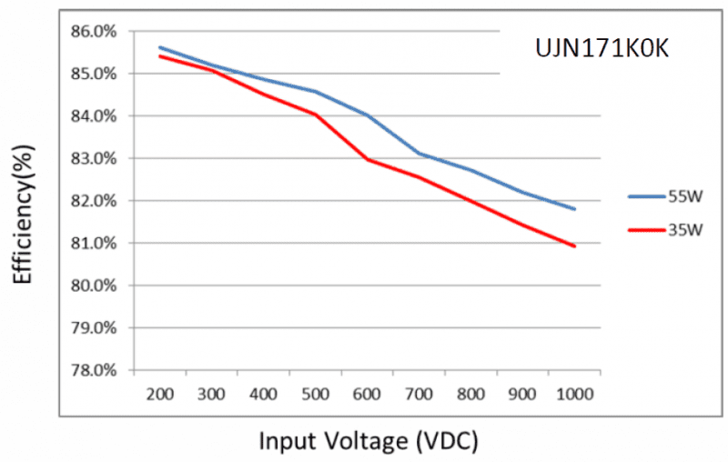 Figure 3. UnitedSiC Utility Power Supply Efficiency vs. Output Power (Vin: 200V to 1000V).
The power level is varied by changing the load on the higher current +12V output, while the +5V output is fixed at 1.25W and -12V output at 8W. The switching frequency is 74kHz. The efficiency for both power levels is greater than 85% at low line, while dropping in the 81% to 82% at high line.
Load and Line Regulation
The high current +12V output is regulated by a TL-431 using a CNY17F opto-coupler to maintain isolation between the primary and secondary side. Graphing the +12V output voltage vs. input voltage in Figure 4, the line regulation is measured at 0.09%, per given power level, and a 0.08% delta in output voltage variance between the two load values.
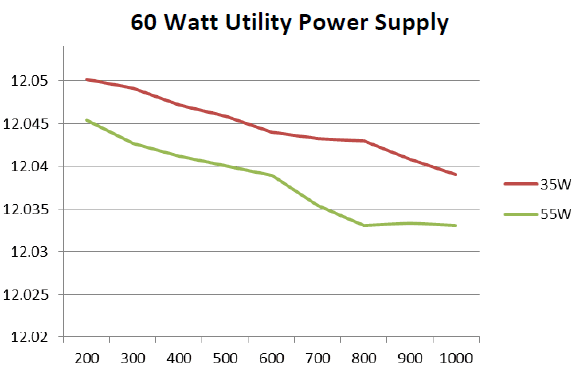 Figure 4. Load and Line Regulation for the +12V output.
Output Ripple
In flyback supplies it is the designer's decision on whether to use LC filters on the output. In this case, LC filters were not used in the initial design. The measured 200mV peak-to-peak of output ripple on the regulated +12V/3A output is shown in Figure 5. As this equates to a ripple percent of 1.67%, and should be acceptable in most ripple requirements, LC filters were not added in subsequent board revisions.
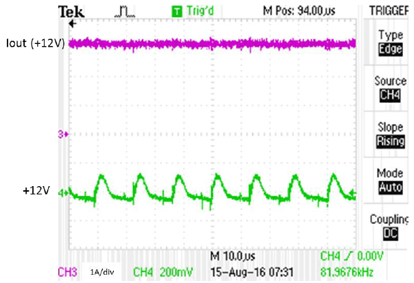 Figure 5. +12V peak-to-peak Ripple is 200mV (Iout = 3A).
Transformer
The flyback transformer (coupled inductor) in this design uses an EPCOS gapped pot core (B65813J160A87). The windings for the primary are 46 turns of 25 AWG. The secondary outputs are +12V (4 turns 18 AWG), -12V (4 turns 22 AWG), +5V (2 turns 22 AWG), and the +12V auxiliary winding (3.5 turns 22 AWG).
To minimize leakage inductance, the first 23 turns of the primarily are wound on to the bobbin, and then the secondary windings are added in a single layer across bobbin. The final 23 turns for the primary are then added. There are many approaches in implementing a magnetic design.
Summary
This application serves to show that a high voltage SiC JFET utilized in a cascode configuration can not only deliver high efficiency to high voltage flyback converters, but it also can simplify the startup circuity, and thus reduce part count, board space and all the corresponding costs.
References
[1] Depletion-mode SiC VJFET Simplifies High Voltage SMPS, PCIM 2012, Nigel Springett and Jeff Casady
[2] Filter Inductor and Flyback Transformer Design for Switching Power Supplies, Lloyd Dixon (Unitrode Design Seminar, 1991)
[3] Switch-Mode Power Supplies, SPICE Simulations and Practical Designs, Christophe Basso (McGraw Hill, 2008)