Kyma Working with IEMN to Reduce Leakage Currents in HV GaN-on-Si HEMTs
Kyma is pleased to be acknowledged for helping scientists at The Institute of Electronics, Microelectronics and Nanotechnology (IEMN) in France to realize high-voltage GaN-on-Si HEMTs with very low leakage currents.
IEMN recently published an open access journal article entitled "GaN-on-silicon high-electron-mobility transistor technology with ultra-low leakage up to 3000V using local substrate removal and AlN ultra-wide bandgap."
Additionally, a summary of that work entitled "High-voltage, ultra-low leakage HEMTs" was published in Compound Semiconductor Magazine in its April/May 2018 Volume.
Those articles describe how IEMN researchers have now achieved GaN-on-Si HEMTs which exhibit a record combination of low leakage current and high blocking voltage. While IEMN had previously attained high standoff voltages of 3kV for GaN-on-Si HEMTs, they had suffered from high leakage currents of 1 mA/mm.
The new 3kV devices reported on showed a 3-order of magnitude reduction in leakage current to less than 1 µA/mm which was enabled by thick AlN materials grown by Kyma within the backside trenches.
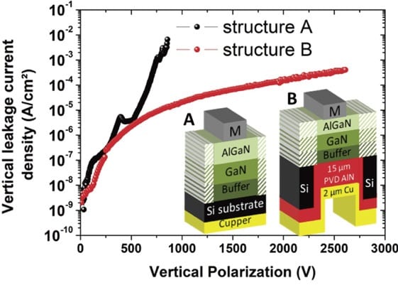
The figure shown above is a copy of Figure 3b from the Applied Physics Express article with caption "AlGaN/GaN epitaxial structures A and B, without and with LSR/backside AlN deposition, respectively."
The following are excerpts from the Compound Semiconductor Magazine article:
"Front-side processing followed, involving: the addition of Ti/Al/Ni/Au ohmic contacts, directly on the AlGaN barrier; device isolation by nitrogen implantation; deposition of a Ni/Au stack on the SiN cap to create metal-insulator-semiconductor structures; and a further deposition of 200 nm of SiN to provide additional passivation. To complete fabrication, the engineers locally etched the substrate up to the AlN nucleation layer, so that silicon is removed up to 50 μm away from the sidewalls, before adding a 15 μm-thick layer of AlN.
The latter step is undertaken by Kyma Technologies. "They had already experience with thick PVD deposition of high resistive AlN," explains Medjdoub, "and deposition in their case can be performed on large wafer diameters."
Kyma's CEO Dr. Keith Evans commented, "We are pleased to assist IEMN researchers in the advancement of their device performances. We believe their results speak well to the excellent capabilities Kyma has developed over the years in advanced plasma vapor deposition technology."
This work demonstrated for the first time GaN-on-Si MISHEMTs with local Si substrate removal under the entire device followed by a low-cost backside deposition of a thick ultra-wide bandgap AlN film. Using an MIS gate structure and the LSR technique combined with a 15-μm-thick AlN layer resulted in state-of-the-art GaN-based HEMTs with remarkably low off-state leakage current (<1µA/mm) beyond 3kV. The comparison of these devices without LSR proves that the drain leakage current flows at the AlN nucleation layer/Si substrate interface.
Furthermore, the significant recovery of the maximum current density after the backside Cu deposition enabled the reduction in self-heating. This work shows that this emerging type of devices could be useful for cost-effective applications requiring breakdown voltages above 3 kV.
Acknowledgments
This work is supported by the French RENATECH network and the ANR project DESTINEE (ANR-16-CE05-0022). This project has received funding from the European Union's Horizon 2020 research and innovation program under grant agreement No. 720527 (Inrel?NPower). The authors would also like to gratefully acknowledge the company EpiGaN for the high material-quality delivery as well as the company Kyma for the thick PVD AlN deposition.


